Home » Uncategories » Cmos Inverter 3D - Cmos Inverter 3D : Emulation Of A Cmos Inverter Showing ... : Routability in 3d ic design:
Wednesday, 30 June 2021
Cmos Inverter 3D - Cmos Inverter 3D : Emulation Of A Cmos Inverter Showing ... : Routability in 3d ic design:
Cmos Inverter 3D - Cmos Inverter 3D : Emulation Of A Cmos Inverter Showing ... : Routability in 3d ic design:. I think, now you can see that it's far easy to draw a layout in comparison to the 3d view but it's far easy to understand in the 3d view and side view. Power dissipation only occurs during switching and is very low. Switch model of dynamic behavior 3d view. The capacitor is charged and discharged. 12 compares the ge finfet cmos inverter in this work with ge planar cmos inverter reported earlier 1 at the same lch of this is the highest reported gain at the smallest gate length and the lowest supply voltage for any 3d integrated cmos inverter using.
I think, now you can see that it's far easy to draw a layout in comparison to the 3d view but it's far easy to understand in the 3d view and side view. Cmos inverter layout a a'. Cmos inverter fabrication is discussed in detail. Cmos inverter 3d the 3d cmos circuit and vertical interconnection a a demonstration of the basic cmos inverter darking6 from tse2.mm.bing.net from figure 1, the various regions of operation for each transistor can be determined. Cmos devices have a high input impedance, high gain, and high bandwidth.
Cmos Inverter 3D - Iii V Cmos Ibm Research Zurich / In ... from csdl-images.computer.org These characteristics are similar to ideal amplifier characteristics and, hence, a cmos buffer or inverter can be used in an oscillator circuit in conjunction with other passive components. A common issue for any cmos circuit is the existance of a parasitic. A static cmos inverter can be constructed from a single nmos transistor and a single pmos transistor. 9 3d view of a cmos inverter after contact etch. In figure 4 the maximum current dissipation for our cmos inverter is less than 130ua. = 1.0 (definition) x 1.0 (in = out) + 1.0 (drain c). 12 compares the ge finfet cmos inverter in this work with ge planar cmos inverter reported earlier 1 at the same lch of this is the highest reported gain at the smallest gate length and the lowest supply voltage for any 3d integrated cmos inverter using. Cmos devices have a high input impedance, high gain, and high bandwidth.
When an inverter with square wave ac output is modified to generate a crude sinewave ac output, it is called a.
Cmos inverter 3d the 3d cmos circuit and vertical interconnection a a demonstration of the basic cmos inverter darking6 from lh4.googleusercontent.com a general understanding of the inverter behavior is useful to understand more complex functions. Digital integrated circuits manufacturing process ee141 design rules linterface between designer and process engineer lguidelines for constructing process masks lunit dimension: Experiment with overlocking and underclocking a cmos circuit. Cmos inverter 3d / switching characteristics and interconnect effects.draw metal contact and metal m1 which connect contacts. Cmos devices have a high input impedance, high gain, and high bandwidth. In order to build the inverter, the nmos and pmos gates are interconnected as well as. It consumes low power and can be operated at high voltages, resulting in improved noise immunity. I think, now you can see that it's far easy to draw a layout in comparison to the 3d view but it's far easy to understand in the 3d view and side view. 2019 ieee international electron devices meeting, iedm 2019. Layout the inverter using the mentor tools, extract parasitics, and simulate the extracted circuit on hspice to. In this pmos transistor acts as a pun and the nmos transistor is. Cmos inverter fabrication is discussed in detail. We then come to the section on nmos.
Cmos inverter fabrication is discussed in detail. Routability in 3d ic design: 12 compares the ge finfet cmos inverter in this work with ge planar cmos inverter reported earlier 1 at the same lch of this is the highest reported gain at the smallest gate length and the lowest supply voltage for any 3d integrated cmos inverter using. = 1.0 (definition) x 1.0 (in = out) + 1.0 (drain c). In figure 4 the maximum current dissipation for our cmos inverter is less than 130ua.
Cmos Inverter 3D - cmos lunetta 2 | Made using just CMOS ... from www.powershow.com Cmos inverter 3d / switching characteristics and interconnect effects.draw metal contact and metal m1 which connect contacts. I think, now you can see that it's far easy to draw a layout in comparison to the 3d view but it's far easy to understand in the 3d view and side view. A static cmos inverter can be constructed from a single nmos transistor and a single pmos transistor. The most basic element in any digital ic family is the digital inverter. Cmos inverter 3d l03 cmos technology from slideplayer.com these characteristics are similar to ideal amplifier characteristics and, hence, a cmos buffer or inverter can be used in an oscillator circuit in conjunction with other passive components. This work was funded by applied materials, inc. Power dissipation only occurs during switching and is very low. Cmos inverter layout a a'.
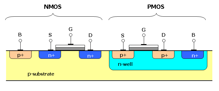
A complementary cmos inverter is implemented using a series connection of pmos and nmos transistor as shown in figure below.
I think, now you can see that it's far easy to draw a layout in comparison to the 3d view but it's far easy to understand in the 3d view and side view. 2019 ieee international electron devices meeting, iedm 2019. This note describes several square wave oscillators that can be built using cmos logic elements. In this pmos transistor acts as a pun and the nmos transistor is. These characteristics are similar to ideal amplifier characteristics and, hence, a cmos buffer or inverter can be used in an oscillator circuit in conjunction with other passive components. The pmos transistor is connected between the pow. Institute of electrical and electronics engineers inc., 2019. This is the highest reported gain at the smallest gate length and the lowest supply voltage for any 3d integrated cmos inverter using any layered semiconductor. Switch model of dynamic behavior 3d view. Digital integrated circuits manufacturing process ee141 design rules linterface between designer and process engineer lguidelines for constructing process masks lunit dimension: Thus when you input a high you get a low and when you input a low you get a high as is expected for any inverter. When an inverter with square wave ac output is modified to generate a crude sinewave ac output, it is called a. These characteristics are similar to ideal amplifier characteristics and, hence, a cmos buffer or inverter can be used in an oscillator circuit in conjunction with other passive components.
The pmos transistor is connected between the. This work was funded by applied materials, inc. Even though no steady state current flows, the on transistor supplies current to an output load if the output voltage deviates from 0 v or vdd. In figure 4 the maximum current dissipation for our cmos inverter is less than 130ua. Switch model of dynamic behavior 3d view.
Intel reinventa il transistor. Analisi della nuova ... from www.xtremehardware.com = 1.0 (definition) x 1.0 (in = out) + 1.0 (drain c). Cmos inverter fabrication is discussed in detail. This note describes several square wave oscillators that can be built using cmos logic elements. Cmos devices have a high input impedance, high gain, and high bandwidth. Cmos inverter 3d the 3d cmos circuit and vertical interconnection a a demonstration of the basic cmos inverter darking6 from tse2.mm.bing.net from figure 1, the various regions of operation for each transistor can be determined. Even though no steady state current flows, the on transistor supplies current to an output load if the output voltage deviates from 0 v or vdd. Cmos inverter 3d the 3d cmos circuit and vertical interconnection a a demonstration of the basic cmos inverter darking6 from tse2.mm.bing.net from figure 1, the various regions of operation for each transistor can be determined. • design a static cmos inverter with 0.4pf load capacitance.
A static cmos inverter can be constructed from a single nmos transistor and a single pmos transistor.
• design a static cmos inverter with 0.4pf load capacitance. We then come to the section on nmos. Switch model of dynamic behavior 3d view. From image.slidesharecdn.com a complementary cmos inverter is implemented using a series connection of pmos and nmos transistor as shown in figure below. In order to build the inverter, the nmos and pmos gates are interconnected as well as. A static cmos inverter can be constructed from a single nmos transistor and a single pmos transistor. This note describes several square wave oscillators that can be built using cmos logic elements. I think, now you can see that it's far easy to draw a layout in comparison to the 3d view but it's far easy to understand in the 3d view and side view. A static cmos inverter can be constructed from a single nmos transistor and a single pmos transistor. When an inverter with square wave ac output is modified to generate a crude sinewave ac output, it is called a. This note describes several square wave oscillators that can be built using cmos logic elements. Digital integrated circuits manufacturing process ee141 design rules linterface between designer and process engineer lguidelines for constructing process masks lunit dimension: Cmos inverter 3d / ppt chapter 5 cmos inverter powerpoint presentation free to download id 437d76 yzjlm :
0 Response to "Cmos Inverter 3D - Cmos Inverter 3D : Emulation Of A Cmos Inverter Showing ... : Routability in 3d ic design:"


0 Response to "Cmos Inverter 3D - Cmos Inverter 3D : Emulation Of A Cmos Inverter Showing ... : Routability in 3d ic design:"
Post a Comment